The S/SC is a device that you attach to the Tandy Color Computer’s cartridge port. It contains a microcontroller that allows access to a SP0256-AL2 speech systhsizer and a AY-3-8913 programable sound generator.
|
Component |
More information |
|---|---|
| Speech/Sound Cartridge | Service Manual, User/Programmers Guide |
| SP0256-AL2 (Speech Processor) | Datasheet, Web Sites |
| AY-3-8913 (Programable Sound Generator) | Datasheet, Web Sites |
| ROM (inside the PIC7040) | Binary, Commented Disassembly (2/20/2022: unfinished) |
| Disk image of S/SC Programs | Direct Link |
| Box | 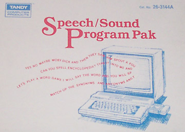 |
| Manual |  |
| Cartridge | 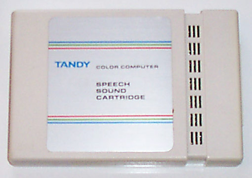 |
A good resource to have is the TMS7000 data manual. The manual can be downloaded here. During this discussion it would be handy to have the schematic (found in the service manual) for reference.
The TMS7000 used in the S/SC has four data ports:
- Port A – Input only. Used to recieve information from the CoCo.
- Port B – Output only. Used as the lower 8 bits of the address bus to the 2k of RAM.
- Port C – Bidirectional. Multifunctional, see below.
- Port D – Bidirectional. Forms an 8 bit data bus used to communicate with the other compenents.
The TMS70x0 has three interrupts:
- INT1 (highest priority) – Signal from the speech chip that it finished speeking, and is ready for a new allophone.
- INT2 (middle priority) – Internal timer interrupt.
- INT3 (Lowest priority) – New data from CoCo.
The TMS7040 has three Registers:
- PC – Program Counter (16 bits)
- SP – Stack Pointer (8 bits) Stack can only exists in first 256 bytes of memory map.
- ST – Status Register (8 bits)
- Bit 7: Carry Bit
- Bit 6: Negative Bit
- Bit 5: Zero Bit
- Bit 4: Global Interrupt Enable/Disable bit
- Other bits unused
Memory Map of the TMS70x0:
| >0000 – >007F | Register File (128 bytes of 8 bit RAM) |
| >0100 – >01FF | Peripherial File (Internal, timer and data port control) |
| >F000 – >FFFF | ROM (internal and/or external) |
Register file:
The register file is real RAM located inside the microcontroller. But it is also acessable as 128 individual registers named R0 thru R127.
For example, the following command:
CLR R22
means clear location 22 (base 10) of the register file. R0 and R1 also have special names: A and B. For example this command:
CLRB
will clear location 1 of the register file.
Peripheral file:
On the TMS7040 a vast majority of the Pheripheral File is unused. Here are the locations that are used:
|
Location in Peripherial File |
Location in Memory Map |
Name |
|---|---|---|
| P0 | >0100 | IOCNT0 – I/O Control |
| P2 | >0102 | T1DATA – Timer 1 Data |
| P3 | >0103 | T1CTL – Timer 1 control |
| P4 | >0104 | APORT – Port A data |
| P6 | >0106 | BPORT – Port B data |
| P8 | >0108 | CPORT – Port C data |
| P9 | >0109 | CDDR – Port C data direction register |
| P10 | >010A | DPORT – Port D data |
| P11 | >010B | DDDR – Port D data direction register |
Peripheral Registers Explained:
IOCNT0: Interrupt Control:
| Bit | 7 | 6 | 5 | 4 | 3 | 2 | 1 | 0 |
| Read | Memory Mode 1 | Memory Mode 0 | INT3 Flag | INT3 Enable | INT2 Flag | INT2 Enable | INT1 Flag | INT1 Enable |
| Write | Memory Mode 1 | Memory Mode 0 | INT3 Clear | INT3 Enable | INT2 Clear | INT2 Enable | INT1 Clear | INT1 Enable |
Memory Mode:
- 00 – Single chip (This is the mode used by the S/SC)
- 01 – Pheripheral Expansion
- 10 – Full Expansion
- 11 – Undefined
INTX Flag: On read this bit tells wether the interrupt had occured
INTX Enable: On read/write this bit determines if an interrupt will cause the interrupt vector to be exectued
INTX Clear: On write, if set to 1, then the flag will be cleared.
T1DATA: Timer 1 data register:
- Read: Current Decrementer Value
- Write: Timer 1 reload register
T1CTL: Timer 1 Control Register:
- Read: Capture Latch Value (current timer value)
- Write:
- Bit 7:
- 0 – Stop timer and holder current value
- 1 – Reload prescaler & decrementer & begin counting
- Bit 6:
- 0 – Counting Source: internal Clock
- 1 – Counting Source: External clock source (Pin A7/EC1)
- Bit 5:
- X – Don’t care
- Bits 4-0:
- Prescale Reload Register
- Bit 7:
APORT: Port A data register:
BPORT: Port B data register:
CPORT: Port C data register:
DPORT: Port D data register:
These 8 bit register hold the value that corespond to that data port.
CDDR: Port C Data direction register:
DDDR: Port D Data direction register:
8 bit registers. Each bit corresponds to a pin on the microcontroller. A 1 makes the pin an output. A 0 makes the pin an input.
The microcontroller communicates with three other devices: 2K of RAM, the Speech Systhsis Chip (SP0256-AL2), and the Programable Sound Generator (AY3-8913).
Port B is A0-A7 for the 2k of RAM
Port C is the internal bus controller:
bit 7 6 5 4 3 2 1 0
    | | | | | | | |
    | | | | | | | + A8 for RAM and BC1 of AY3-8913
    | | | | | | +-- A9 for RAM
    | | | | | +---- A10 for RAM
    | | | | +------ R/W* for RAM and BDIR for AY3-8913
    | | | +-------- CS* for RAM
    | | +---------- ALD* for SP0256
    | +------------ CS* for AY3-8913
    +-------------- BUSY* for host CPU (connects to a latch)
* – Active low
Port D is the 8-bit data bus.
Port C is where all the action is. The status of thoes lines control what chip the microcontroller is talking to. Using this arrangement the microcontroller can:
- Put data into the RAM.
- Port C, pin 4: Low
- Port C, pin 3: Low for wirting
- Read data from the RAM.
- Port C, pin 4: Low
- Port C, pin 3: High for reading
- Load an allophone into the speech chip.
- Port C, pin 5: Low
- Load data into a PSG register
- Read data from a PSG register
- See data sheets for how to access the PSG